Boolean Algebra & Logic Circuits (Cambridge (CIE) A Level Computer Science): Exam Questions

Exam code: 9618

2 hours25 questions
1a
3 marks

The truth table for a logic circuit is shown.

INPUT

OUTPUT

A

B

C

D

T

0

0

0

0

0

0

0

0

1

1

0

0

1

0

0

0

0

1

1

1

0

1

0

0

0

0

1

0

1

0

0

1

1

0

0

0

1

1

1

0

1

0

0

0

0

1

0

0

1

1

1

0

1

0

0

1

0

1

1

1

1

1

0

0

0

1

1

0

1

1

1

1

1

0

0

1

1

1

1

1

Write the Boolean logic expression that corresponds to the given truth table as the sum-of-products.

1b
2 marks

Complete the Karnaugh map (K-map) for the given truth table.
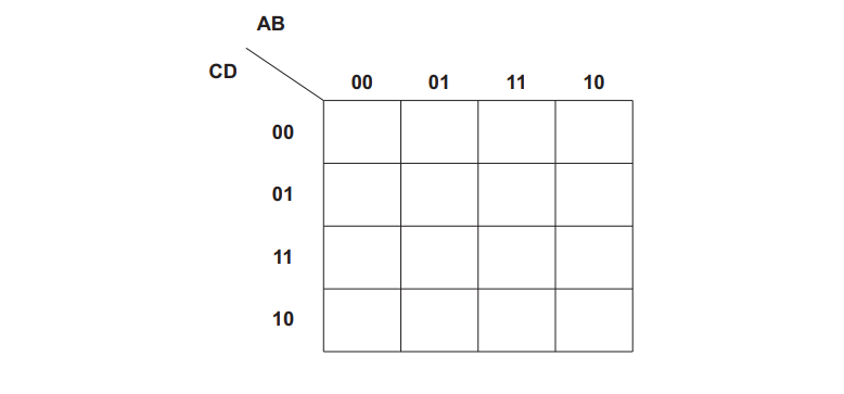
4x4 Karnaugh map with labels AB and CD; columns marked 00, 01, 11, 10, and rows marked 00, 01, 11, 10, with empty cells.
1c
2 marks

Draw loop(s) around appropriate group(s) in the K-map to produce an optimal sum-of-products.

1d
3 marks

(i) Write the Boolean logic expression from your answer to part (c) as the simplified sum-of-products.

(2)

(ii) Use Boolean algebra to write your answer to part (d)(i) in its simplest form.

(1)

2a
3 marks

The truth table for a logic circuit is shown.

INPUT

OUTPUT

A

B

C

D

X

0

0

0

0

0

0

0

0

1

1

0

0

1

0

1

0

0

1

1

0

0

1

0

0

0

0

1

0

1

1

0

1

1

0

1

0

1

1

1

0

1

0

0

0

0

1

0

0

1

1

1

0

1

0

1

1

0

1

1

0

1

1

0

0

0

1

1

0

1

1

1

1

1

0

Write the Boolean logic expression that corresponds to the given truth table as the sum‑of‑products.

2b
2 marks

Complete the Karnaugh map (K‑map) for the given truth table.

2c
2 marks

Draw loop(s) around appropriate group(s) in the K‑map to produce an optimal sum‑of‑products.

2d
2 marks

Write the Boolean logic expression from your answer to part (c) as the simplified sum‑of‑products.

3a
2 marks

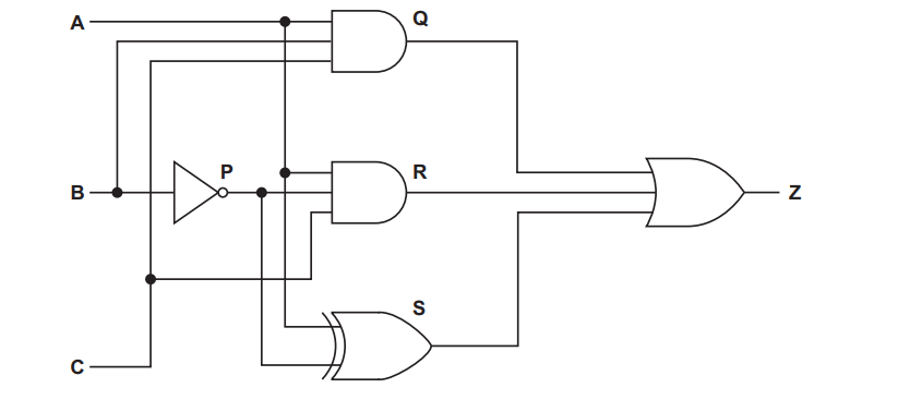
The diagram shows a logic circuit.

Logic circuit diagram with inputs A, B, C. Includes AND, OR, NOT gates; Q, R, S outputs lead to Z. P denotes NOT gate output.

Write the Boolean expression that corresponds to the logic circuit as a sum-of-products.

3b
5 marks

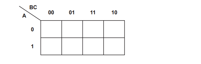
Complete the Karnaugh map (K-map) for the Boolean expression:

A¯.B¯.C¯ + A¯.B¯.C + A.B¯.C¯ + A.B¯.C + A.B.C¯ + A.B.C

A blank 2x4 Karnaugh map with labels A, BC, rows 0, 1, and columns 00, 01, 11, 10, used for simplifying Boolean expressions.

(2)

(ii) Draw loop(s) around appropriate group(s) in the K-map to produce an optimal sum-of-products.

(2)

(iii) Write the Boolean expression from your answer to part (c)(ii) as a simplified sum-of-products.

(1)

4a
2 marks

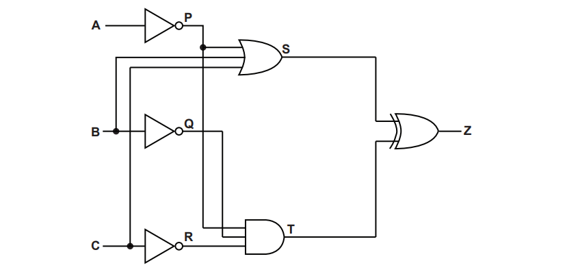
The diagram shows a logic circuit.

Logic circuit diagram showing inputs A, B, C through NOT gates, combining in AND, OR, and final OR gate, outputting to Z.

Write the Boolean expression that corresponds to the logic circuit as a sum-of-products.

4b
5 marks

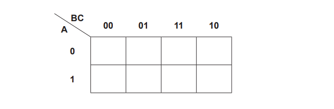
(i) Complete the Karnaugh map (K-map) for this Boolean expression:

A¯.B¯.C¯ + A¯.B.C¯+ A¯.B.C + A.B¯.C¯–  + A.B.C¯+ A.B.C

A blank Karnaugh map with two rows and four columns; labelled with variables A, B, and C. Column headers: 00, 01, 11, 10. Row headers: 0, 1.

(2)

(ii) Draw loop(s) around appropriate group(s) in the K-map to produce an optimal sum-of-products.

(2)

(iii) Write the Boolean expression from your answer to part c(ii) as a simplified sum-of-products.

(1)

5a
3 marks

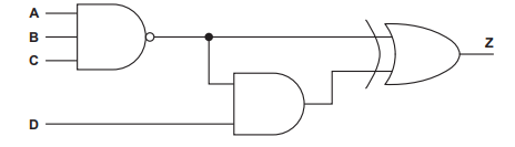
This diagram represents a logic circuit.

Logic circuit diagram with an AND gate taking inputs A, B, C, a NOT gate, another AND gate with input D, and an OR gate producing output Z.

Complete the truth table for the given logic circuit.

A

B

C

D

Working space

Z

0

0

0

0

0

0

0

1

0

0

1

0

0

0

1

1

0

1

0

0

0

1

0

1

0

1

1

0

0

1

1

1

1

0

0

0

1

0

0

1

1

0

1

0

1

0

1

1

1

1

0

0

1

1

0

1

1

1

1

0

1

1

1

1

5b
3 marks

Simplify the given Boolean expression using Boolean algebra.
Show your working.

Boolean equation with NOT A, AND B, AND C, AND D plus NOT A, AND B, AND C, AND NOT D plus NOT A, AND B, AND NOT C, AND D.
6a
1 mark

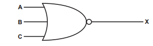
This logic circuit represents the Boolean expression: X = A + B + C¯

Logic gate diagram with three inputs labelled A, B, C, leading into a NOR gate, producing a single output labelled X.

Complete this truth table for the given logic circuit.

A

B

C

X

0

0

0

0

0

1

0

1

0

0

1

1

1

0

0

1

0

1

1

1

0

1

1

1

6b
1 mark

Apply De Morgan’s laws to the expression: X = A + B + C¯

X = ...................................................................................

6c
3 marks

Simplify the following expression using Boolean algebra.

Show all the stages in your simplification.

T = X.Y.Z + X.Y.¯Z + X¯

7
3 marks

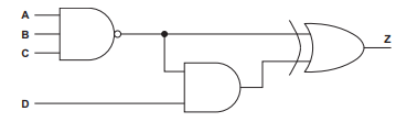
This diagram represents a logic circuit.

Logic circuit diagram featuring a three-input NAND gate, a two-input AND gate, a two-input OR gate, and four inputs labelled A, B, C, D leading to output Z.

Simplify the given Boolean expression using Boolean algebra.
Show your working.

Y = A¯.B¯.C¯.D¯ + A¯.B¯.C.D¯ + A¯.B.C¯.D¯ + A¯.B.C.D¯

8
2 marks

A half adder is a logic circuit with two inputs, A and B, and two outputs, E and F.

The completed truth table for the half adder is shown.

INPUT

OUTPUT

A

B

E

F

0

0

0

0

0

1

1

0

1

0

1

0

1

1

0

1

State the purpose of each of the two outputs E and F.

9
3 marks

A logic circuit has two inputs, A and B, and two outputs, E and F.

The two outputs are given by these logic expressions:

E = A XOR B

F = A AND B

(a) Complete the truth table for this logic circuit.

INPUT

OUTPUT

A

B

E

F

0

0

0

1

1

0

1

1

(2)

(b) State the name of this logic circuit.

(1)

10
2 marks

An SR flip-flop is a logic circuit built from two logic gates that are connected together. Flip-flops are used inside a computer as data storage elements.

(i) State the purpose of one flip-flop.

(1)

(ii) A computer stores one byte of data in Static RAM (SRAM), which is built from flip-flops.

State the number of flip-flops that are needed to store this one byte.

(1)

11
4 marks

A logic circuit has two inputs, A and B, and two outputs, E and F.

The circuit uses two intermediate signals, P and Q, which are given by these logic expressions:

P = A NAND B

Q = A OR B

The two outputs are given by these logic expressions:

E = P AND Q

F = NOT P

(a) Complete the truth table for this logic circuit.

Show your working in the working space columns.

INPUT

Working space

OUTPUT

A

B

P

Q

E

F

0

0

0

1

1

0

1

1

(3)

(b) State the name of this logic circuit.

(1)

12
3 marks

An SR flip-flop is built from two NOR gates that are connected together as follows.

  • The output of the first NOR gate is Q.

  • The output of the second NOR gate is NOT Q.

  • The two inputs to the first NOR gate are R and NOT Q.

  • The two inputs to the second NOR gate are S and Q.

The flip-flop is storing the value Q = 1, so NOT Q = 0.

Each pair of input values in the table is applied to the flip-flop while it is storing Q = 1. The first row has been completed for you.

Complete the table to show the values of Q and NOT Q produced by each of the other three pairs of input values.

S

R

Q

NOT Q

1

0

1

0

0

0

0

1

1

1

13
4 marks

A factory uses an SR flip-flop built from two NOR gates to store the state of a temperature alarm.

  • Input S is connected to a temperature sensor. S becomes 1 when the temperature rises above the safe limit.

  • Input R is connected to a reset button. R is 1 only while an operator holds the button down.

  • Output Q drives the alarm. The alarm sounds when Q = 1.

Before the first event the flip-flop is storing Q = 0, so NOT Q = 1.

The four events in the table happen one after the other, in the order shown.

Complete the table to give the value of output Q after each event.

Event

S

R

Q after the event

The temperature rises above the safe limit

1

0

The temperature returns to a safe value

0

0

The operator holds down the reset button

0

1

The operator releases the reset button

0

0

14
2 marks

A full adder is a logic circuit that adds three single binary digits, A, B and C.

The circuit has two outputs. Output Y is the sum and output Z is the carry.

Complete the truth table for the full adder.

INPUT

OUTPUT

A

B

C

Y

Z

0

0

0

0

0

1

0

1

0

0

1

1

1

0

0

1

0

1

1

1

0

1

1

1

15
3 marks

A logic circuit has three inputs, A, B and C, and two outputs, Y and Z.

The completed truth table for the logic circuit is shown.

INPUT

OUTPUT

A

B

C

Y

Z

0

0

0

0

0

0

0

1

1

0

0

1

0

1

0

0

1

1

0

1

1

0

0

1

0

1

0

1

0

1

1

1

0

0

1

1

1

1

1

1

(a) State the name of this logic circuit.

(1)

(b) State the purpose of each of the two outputs Y and Z.

(2)

16
4 marks

A logic circuit has three inputs, A, B and C, and two outputs, Y and Z.

The circuit uses three intermediate signals, P, Q and R, which are given by these logic expressions:

P = A XOR B

Q = A AND B

R = P AND C

The two outputs are given by these logic expressions:

Y = P XOR C

Z = Q OR R

(a) Complete the truth table for this logic circuit.

Show your working in the working space columns.

INPUT

Working space

OUTPUT

A

B

C

P

Q

R

Y

Z

0

0

0

0

0

1

0

1

0

0

1

1

1

0

0

1

0

1

1

1

0

1

1

1

(3)

(b) State the name of this logic circuit.

(1)

17
2 marks

A student is learning the rules of Boolean algebra.

Complete the table by writing the simplest form of each Boolean expression.

Expression

Simplest form

A.1

A+0

A.A¯

A+A¯

18
2 marks

A logic circuit has the inputs A, B and C, and the output Z.

The completed Karnaugh map (K-map) for the output Z is shown. The columns are labelled with the values of BC and the rows are labelled with the values of A.

BC →
A ↓

00

01

11

10

0

0

0

1

0

1

1

1

1

1

Write the Boolean expression for the output Z as a simplified sum-of-products.

19
3 marks

A logic circuit has the inputs A, B, C and D, and the output X.

The completed Karnaugh map (K-map) for the output X is shown. The columns are labelled with the values of AB and the rows are labelled with the values of CD.

AB →
CD ↓

00

01

11

10

00

0

0

1

0

01

0

0

1

0

11

1

0

0

1

10

1

0

0

1

Write the Boolean logic expression for the output X as the optimal sum-of-products.

State the number of squares in the largest loop you have used.

20
3 marks

A logic circuit produces the output Z.

Z=(A+B).(A+B¯)

Simplify this expression using Boolean algebra.

Show your working.

21
4 marks

A logic circuit has the inputs A, B, C and D, and the output T.

The completed Karnaugh map (K-map) for the output T is shown. The columns are labelled with the values of AB and the rows are labelled with the values of CD.

AB →
CD ↓

00

01

11

10

00

0

0

1

1

01

0

0

0

0

11

0

1

1

0

10

0

0

1

1

A student has used this K-map and has written the following sum-of-products for T.

T=A.C¯.D¯+A.C.D¯+B.C.D

The student's expression gives the correct output for every combination of inputs, but it is not the optimal sum-of-products.

Explain why the student's expression is not the optimal sum-of-products, and write the optimal sum-of-products for T.

22
4 marks

The truth table for a logic circuit is shown.

INPUT

OUTPUT

A

B

C

X

0

0

0

1

0

0

1

1

0

1

0

0

0

1

1

0

1

0

0

0

1

0

1

0

1

1

0

1

1

1

1

1

(i) Write the Boolean expression that corresponds to the given truth table as a sum-of-products.

(2)

(ii) Use Boolean algebra to write your answer to part (i) in its simplest form.

Show your working.

(2)

23
1 mark

A logic circuit produces the output X.

X=A.B.C¯

Apply De Morgan's laws to this expression.

24
2 marks

A logic circuit produces the output Y.

Y=A¯+B¯

Apply De Morgan's laws to this expression and write the result in its simplest form.

25
3 marks

A logic circuit produces the output T.

T=A+B¯+A+B¯¯

Simplify this expression using Boolean algebra, including De Morgan's laws.

Show your working.